
LM2596 Regulator
LM2596
Texas Instruments · Serie LM259x
Galería
Productos relacionados
Ver todos


Descripción
LM2596 Technical Guide: 3A Simple Switcher Step-Down Voltage Regulator
The LM2596 isn't just a regulator; it’s a late-90s statement of intent that refuses to die. We are looking at a non-synchronous buck DC-DC converter with an integrated power transistor, designed for those who value simplicity over the extreme efficiency of modern 1 MHz converters. Its fixed switching frequency of 150 kHz allows for smaller filtering components than low-frequency regulators, though today that figure seems conservative compared to newer BySMax options.
⚠️ Survival Limits Ignoring these values is signing your PCB's death warrant:
- Maximum Input Voltage ($V_{IN}$): 45 V (Absolute) / 40 V (Operating).
- ON/OFF Pin Voltage: 25 V.
- Current Limit (Peak): 6.9 A (Typical at $V_{IN} = 12 V$, but don't get overconfident).
- Maximum Junction Temperature ($T_{J}$): 150 °C.
Pinout and Physical Reference
Available in TO-220 (for those who still believe in massive heatsinks) and TO-263 (for surface mount soldering with a solid copper plane).
| No. | Pin | I/O | Technical Description |
|---|---|---|---|
| 1 | $V_{IN}$ | I | Supply Input. Requires mandatory low ESR bypass capacitor. |
| 2 | Output | O | Internal switching node. Duty cycle $D = V_{OUT}/V_{IN}$. |
| 3 | Ground | - | Circuit Ground. |
| 4 | Feedback | I | Control loop input. Output voltage sensing. |
| 5 | ON/OFF | I | Shutdown logic. < 1.3 V enables; > 1.3 V disables (80 µA standby). |
Laboratory Specifications
| Parameter | Typical Range | Unit | Notes |
|---|---|---|---|
| Oscillation Frequency | 150 (±15%) | kHz | Internally fixed. |
| Reference Voltage ($V_{REF}$) | 1.23 (±2%) | V | For the adjustable version. |
| Efficiency (5V Out) | 80 | % | With $V_{IN} = 12 V$ and $I_{LOAD} = 3 A$. |
| Standby Current | 80 | µA | Typical when pin 5 is pulled high. |
Applied Engineering
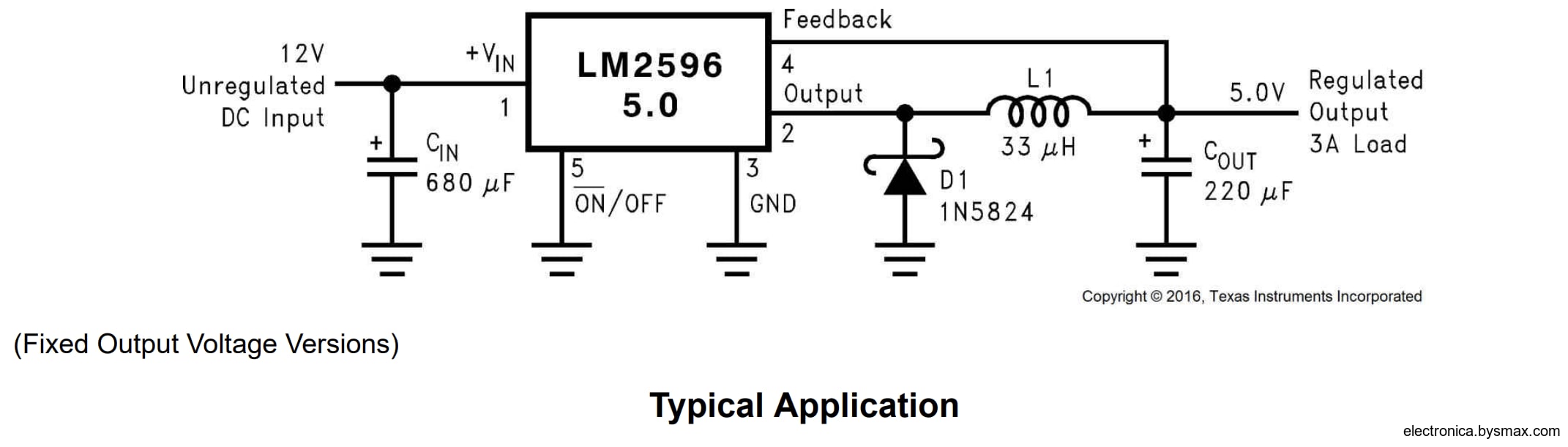
1. Fixed Voltage Configuration and Output Filtering
[INSERTAR IMAGEN: Figure 9-10. Fixed Output Voltage Version]
This is the standard design. The "catastrophe" prevented by the input capacitor ($C_{IN}$) of 680 µF is the collapse of the input voltage due to current transients. If the output capacitor ($C_{OUT}$) ESR is too low (as seen in certain ceramics), the feedback loop becomes unstable and the regulator will oscillate like there's no tomorrow.
2. Delayed Startup (Primitive Soft-start)

The LM2596 lacks a dedicated soft-start pin. This circuit utilizes the $R/C$ time constant on the ON/OFF pin to prevent the regulator from attempting to deliver full current instantly while the input source is still stabilizing. Useful for "weak" power supplies that trigger protection during startup current spikes.
3. Inverting Regulator with Undervoltage Lockout
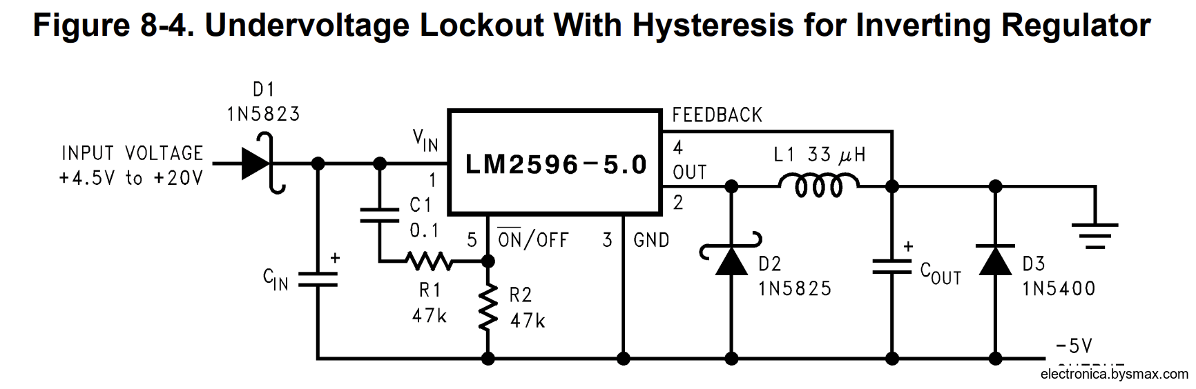
An applied engineering gem. By "floating" the IC's ground pin to the negative output, the regulator sees the sum of $|V_{IN}| + |V_{OUT}|$. The circuit with $Z1$ and $Q1$ adds hysteresis: the system won't start until $V_{IN}$ reaches a safe level, preventing the regulator from getting stuck in an inefficient linear conduction state or erratic switching during power-up.
4. Post-Regulation Ripple Filtering

Even at 150 kHz, ripple can be unacceptable for sensitive analog stages. Using an external LC filter ($L_{2} \approx 20 \mu H$) outside the feedback loop can reduce output ripple to less than 10 mV without compromising system stability.
BySMax Selection Criteria
The LM2596 remains in our inventory because it is a "tank". While more efficient and compact options exist (such as the LMR51430), the LM2596 forgives layout errors that would destroy modern components, and its ease of implementation with only four external components makes it unbeatable for rapid industrial-grade prototyping.