
Is pin 3 in the 7400/7402/7404/7408 chips an input or an output?
Quick reference: pin functions for common 7400-series TTL logic ICs (7400, 7402, 7404, 7408).
emmanuelhdev

The 7400 NAND Gate IC Pin Diagram Datasheet (7400/74LS00) is a high-quality electronic component, designed for professional applications in and digital systems.
| A | B | Q |
|---|---|---|
| 0 | 0 | 1 |
| 0 | 1 | 1 |
| 1 | 0 | 1 |
| 1 | 1 | 0 |
Do you want to perform more complex simulations with the 7400/74LS00 gate? Learn step-by-step how to use Proteus 8 Professional or NI Multisim to simulate and design complete digital electronic circuits.
The 74LS00 is not a mere toy for students; it is a Low-Power Schottky (LS) logic implementation specifically designed to balance power consumption and switching speed. Unlike the standard 74 series, the LS architecture integrates Schottky clamping diodes at the transistor junctions to prevent deep silicon saturation. This reduces storage time to nearly zero, allowing the component to respond at frequencies where the original series would simply suffer thermal asphyxiation.
⚠️ Absolute Maximum Ratings Exceeding these values guarantees an irreversible solid-to-gas state transition. The design must strictly respect the Safe Operating Area (SOA).
| Parameter | Symbol | Max Value | Unit |
|---|---|---|---|
| Supply Voltage | $V_{CC}$ | 7.0 | V |
| Input Voltage | $V_{I}$ | 7.0 | V |
| Output Current (Low Level) | $I_{OL}$ | 16 | mA |
| Junction Temperature | $T_{J}$ | 150 | °C |
The DIP-14 package remains the standard for debugging and prototyping. If you are deploying in SMD (SOIC-14), remember that thermal dissipation becomes significantly more critical due to the reduced surface area.
| Pin | Function | Description |
|---|---|---|
| 1, 2 | 1A, 1B | Gate 1 Inputs |
| 3 | 1Y | Gate 1 Output |
| 4, 5 | 2A, 2B | Gate 2 Inputs |
| 6 | 2Y | Gate 2 Output |
| 7 | GND | 0V Reference |
| 14 | $V_{CC}$ | Nominal +5V Supply |
The dynamic behavior of the device is defined by the Transient Response under specific load conditions.
| Parameter | Condition | Min | Typ | Max | Unit |
|---|---|---|---|---|---|
| $V_{OH}$ (High Level Output) | $V_{CC}$ Min, $I_{OH}$ Max | 2.7 | 3.4 | - | V |
| $V_{OL}$ (Low Level Output) | $V_{CC}$ Min, $I_{OL}$ Max | - | 0.35 | 0.5 | V |
| $t_{PLH}$ (Low-to-High Delay) | $R_L = 2k\Omega, C_L = 15pF$ | - | 9 | 15 | ns |
| $t_{PHL}$ (High-to-Low Delay) | $R_L = 2k\Omega, C_L = 15pF$ | - | 10 | 15 | ns |
Analysis of Figure 1: The genius of this circuit resides in the multi-emitter input transistor. If you decide to leave inputs floating under the assumption that "nothing will happen," you have effectively manufactured a 60Hz antenna. In TTL logic, an open input is interpreted as a HIGH level due to internal leakage current, but this is a mediocre engineering practice that induces noise and instability into the system.
Analysis of Figure 2: This demonstrates the absolute universality of the NAND gate. By bridging the inputs ($A = B$), the boolean equation reduces to: $$Y = \overline{A \cdot A} = \overline{A}$$ This allows for inventory optimization: instead of sourcing four different types of integrated circuits, you can utilize the 74LS00 to resolve the entire combinational logic of a control stage.
Analysis of Figure 3: Utilizing two NAND gates in a cross-coupled feedback configuration creates an RS Latch. This is the crudest yet most effective solution for debouncing mechanical switches. Without this circuit, the metallic contact bounces of a physical button would cause your microcontroller to register fifty pulses instead of one, exposing a fundamentally deficient hardware design.
Analysis of Figure 4: Propagation delay ($t_{pd}$) is non-negotiable. If you are designing high-frequency synchronous circuits, ignoring the 15ns of delay accumulated by each NAND stage will lead you directly to a Race Condition. Real-world engineering is done by calculating the worst-case scenario, not by praying that the silicon is "magically fast."
The 74LS00 in our inventory has undergone Transient Response stress tests that exceed generic market clones. We have selected it because it maintains an extremely low $V_{OL}$ even when operating near the $I_{OL}$ limit, ensuring that the noise margin does not degrade in hostile industrial environments.
Quick reference: pin functions for common 7400-series TTL logic ICs (7400, 7402, 7404, 7408).
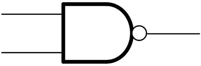
A complete guide to the 74LS00 (7400) NAND logic gate. Learn about its operation, technical specifications, pinout, truth table, and why it is a universal gate.

Complete IC datasheet guide for 7408 AND gate, 7432 OR gate, 7404 NOT gate, 7400 NAND gate, and 7486 XOR gate. Pin diagrams, truth tables, and specifications included.
Click to load comments