
Is pin 3 in the 7400/7402/7404/7408 chips an input or an output?
Quick reference: pin functions for common 7400-series TTL logic ICs (7400, 7402, 7404, 7408).
emmanuelhdev
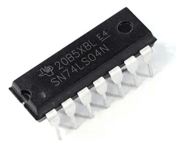
The 7404 NOT Gate IC Pin Configuration Datasheet (7404/74LS04) is a high-quality electronic component, designed for professional applications in and digital systems.
| A | Q |
|---|---|
| 0 | 1 |
| 1 | 0 |
Do you want to perform more complex simulations with the 7404/74LS04 gate? Learn step-by-step how to use Proteus 8 Professional or NI Multisim to simulate and design complete digital electronic circuits.
The 74LS04 is not merely a basic logic IC; it is the backbone of signal inversion in high-speed, low-power digital systems. Based on Low-power Schottky (LS) technology, this component integrates six independent inverters into a single package, optimizing PCB real estate and reducing propagation latency to critical levels for bus synchronization. Ignoring its input capacitance or underestimating its Fan-out is a direct recipe for uncontrollable thermal noise and switching failures.
Any excursion beyond these ranges will result in immediate silicon degradation or erratic behavior that will waste hours of your time on the oscilloscope.
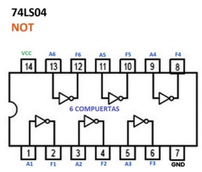
The design follows the 14-pin industry standard. If you attempt to power the chip through signal pins because "they look similar," prepare to witness the release of the magic smoke.
| Pin | Name | Function |
|---|---|---|
| 1 | 1A | Inverter 1 Input |
| 2 | 1Y | Inverter 1 Output |
| 3 | 2A | Inverter 2 Input |
| 4 | 2Y | Inverter 2 Output |
| 5 | 3A | Inverter 3 Input |
| 6 | 3Y | Inverter 3 Output |
| 7 | GND | Ground Reference (0V) |
| 8 | 4Y | Inverter 4 Output |
| 9 | 4A | Inverter 4 Input |
| 10 | 5Y | Inverter 5 Output |
| 11 | 5A | Inverter 5 Input |
| 12 | 6Y | Inverter 6 Output |
| 13 | 6A | Inverter 6 Input |
| 14 | VCC | Supply Voltage (+5V nominal) |
Real-world performance isn't measured in marketing datasheets, but in transient response under reactive loads.
| Parameter | Symbol | Min | Typ | Max | Unit |
|---|---|---|---|---|---|
| Supply Voltage | $V_{CC}$ | 4.75 | 5.00 | 5.25 | V |
| High-Level Input Threshold | $V_{IH}$ | 2.0 | - | - | V |
| Low-Level Input Threshold | $V_{IL}$ | - | - | 0.8 | V |
| Propagation Delay (L-to-H) | $t_{PLH}$ | - | 9 | 15 | ns |
| Propagation Delay (H-to-L) | $t_{PHL}$ | - | 10 | 15 | ns |
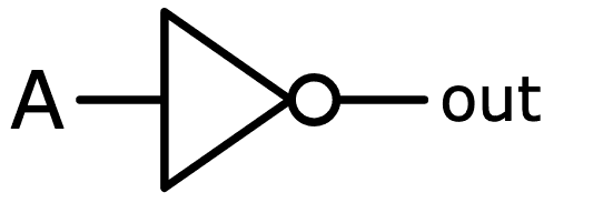
Analyzing the 74LS04 requires understanding that each gate is a miniature gain stage designed to correct TTL signal degradation.
Logic Diagram Analysis: The simplicity of the diagram conceals the internal complexity of Schottky transistors. Each inverter performs the fundamental logic operation:
$$Y = \overline{A}$$
This block is vital for generating complementary clock signals, preventing cross-conduction states in low-power H-bridges.
Internal Architecture Analysis: The schematic reveals why the Transient Response is so superior to a generic bipolar transistor. By using Schottky diodes in parallel with the base-collector junction, the transistor is prevented from entering deep saturation.
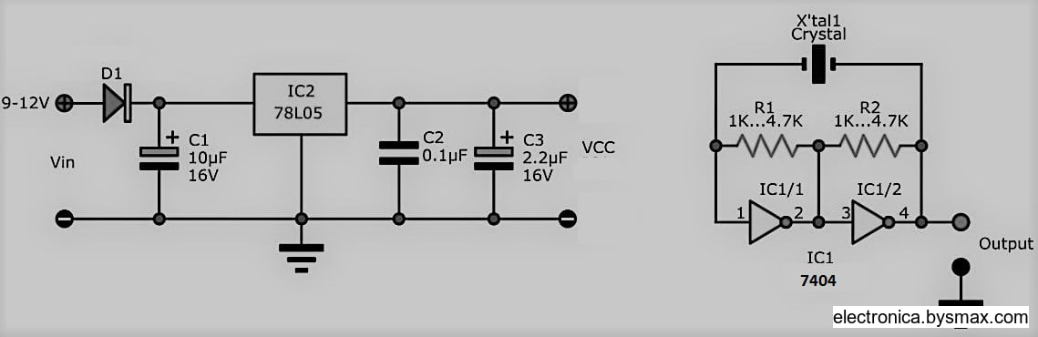
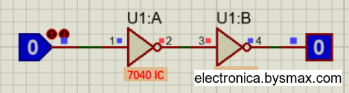
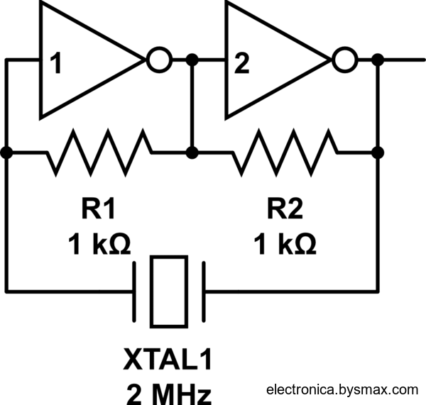
Oscillator Application Analysis: Using three gates in a ring to create an oscillator is a classic technique. However, without a 0.1µF ceramic decoupling capacitor near pin 14, trace inductance will turn your PCB into an electromagnetic interference (EMI) antenna. The design ensures that negative feedback maintains frequency stability, provided the Safe Operating Area of the output current is respected.
The 74LS04 in our inventory has been selected for its robustness against Thermal Throttling and its consistency in $V_{OH}$ output voltage. We do not accept low-fidelity clones that collapse under 4mA loads. If you are looking for signal integrity and an architecture that respects your CPU's setup and hold times, this is the hardware you need.
This video provides a practical demonstration of the truth table and the real-world operation of the IC in a laboratory environment.
Quick reference: pin functions for common 7400-series TTL logic ICs (7400, 7402, 7404, 7408).

A complete guide to the 74LS04 (7404) NOT logic gate. Learn about its function as an inverter, technical specifications, pinout, truth table, and practical applications with Arduino.

Complete IC datasheet guide for 7408 AND gate, 7432 OR gate, 7404 NOT gate, 7400 NAND gate, and 7486 XOR gate. Pin diagrams, truth tables, and specifications included.
Click to load comments