
Is pin 3 in the 7400/7402/7404/7408 chips an input or an output?
Quick reference: pin functions for common 7400-series TTL logic ICs (7400, 7402, 7404, 7408).
emmanuelhdev

The 7408 AND Gate IC Datasheet Pin Diagram (7408/74LS08) is a high-quality electronic component, designed for professional applications in and digital systems.
| A | B | Q |
|---|---|---|
| 0 | 0 | 0 |
| 0 | 1 | 0 |
| 1 | 0 | 0 |
| 1 | 1 | 1 |
Do you want to perform more complex simulations with the 7408/74LS08 gate? Learn step-by-step how to use Proteus 8 Professional or NI Multisim to simulate and design complete digital electronic circuits.
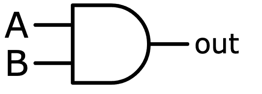
The 74LS08 (also known as 7408) is a TTL integrated circuit that contains four independent two-input AND logic gates. It is typically powered with +5V (4.75–5.25V), and each gate performs the Boolean operation Y = A·B: the output is "1" only if both inputs are "1". In any other case, the output is "0".
This component from the 74LS (Low-power Schottky) series is known for its ease of use in breadboards and digital projects involving Arduino, microcontrollers, and telecommunication systems where combined AND logic functions are needed.
The 74LS08 is a quad low-power AND gate (LS series). Its main features include:
This allows it, for example, to drive LEDs or simple loads directly from the output, making it ideal for basic digital electronics projects.
Each AND gate inside the 74LS08 operates with a simple logic: the output is "1" only when both inputs are "1". This Boolean operation is expressed as Y = A·B.
Truth table for each AND gate:
| Input A | Input B | Output Y |
|---|---|---|
| 0 | 0 | 0 |
| 0 | 1 | 0 |
| 1 | 0 | 0 |
| 1 | 1 | 1 |
Internal operation: Each gate is based on low-power Schottky TTL technology, using bipolar transistors and Schottky devices to switch quickly with a typical delay of ~10 ns.
The 74LS08 comes in a 14-pin DIP package with the following configuration:
Note: The full pin diagram is shown in the datasheet from the previous section.
| Specification | Parameter (74LS08) |
|---|---|
| Logic Function | AND |
| Number of AND gates | 4 (quad) |
| Inputs per gate | 2 |
| Supply Voltage | 4.75 – 5.25 V |
| Technology | TTL 74LS family (LS-TTL) |
| Output Current (I<sub>OL</sub>) | up to 16 mA (low level) |
| Output Current (I<sub>OH</sub>) | –0.8 mA (high level) |
| Max. Speed (f<sub>max</sub>) | ~35 MHz |
| Typical Delay (t<sub>pd</sub>) | ~10 ns (propagation) |
| Operating T<sub>range</sub> | 0 °C to 70 °C |
In addition to the 74LS08 (TTL LS), there are variants compatible with different technologies:
The 74LS08 is very useful in digital prototypes where hardware logic combinations are required:
Example circuit: Two push-buttons (S1, S2) with pull-down resistors (R1, R2) control the A and B inputs of the gate. The Y output drives an LED with a resistor (R3). The LED only turns on when both buttons are pressed.
Circuit connections:
What gate is the 7408? The 7408 (also 74LS08) is an integrated circuit with four two-input AND gates. It contains four independent AND logic gates.
What is the truth table for the 74LS08? Each 7408 AND gate follows the table: A=0,B=0 → Y=0; 0,1→0; 1,0→0; 1,1→1. It only outputs "1" when A=1 and B=1.
What voltage does the 74LS08 operate at? It operates at a standard TTL voltage, typically 5V (range 4.75–5.25V). It does not work directly at 3.3V. For 3.3V, it's better to use a 74HCT08.
Can I use a 74HC08 instead of a 74LS08? Yes. The 74HC08 is CMOS and works between 2V and 6V. In a 5V system, it will function as a functional equivalent, although it provides less output current (5.2 mA) compared to the LS version (16 mA).
How do I connect the 74LS08 on a breadboard with Arduino? Connect VCC=+5V (pin 14) and GND=0V (pin 7). Use the outputs to turn on LEDs or trigger Arduino pins, and connect inputs to buttons or digital signals from the Arduino. Add pull-down/up resistors if you leave inputs unconnected.
What do SN74LS08, 74HC08, etc., mean? The prefix indicates the logic family: 74LS08 is TTL Low-Power Schottky; 74HC08 is High-speed CMOS; 74HCT08 is CMOS with TTL-compatible inputs. All perform the same AND function but differ in voltage, speed, and consumption.
References: Information is based on official datasheets from Texas Instruments and technical sources to ensure accuracy.
Quick reference: pin functions for common 7400-series TTL logic ICs (7400, 7402, 7404, 7408).

A complete guide to the 74LS08 (7408) logic gate - its operation, technical specifications, pinout, practical applications, and circuit examples for projects with Arduino.

Complete IC datasheet guide for 7408 AND gate, 7432 OR gate, 7404 NOT gate, 7400 NAND gate, and 7486 XOR gate. Pin diagrams, truth tables, and specifications included.
Aprende a construir un sumador de 4 bits con display de 7 segmentos en Proteus usando compuertas lógicas. Incluye sumador-restador, tabla de verdad y simulación paso a paso.
Aprende a construir un sumador de 4 bits con display de 7 segmentos en Proteus usando compuertas lógicas. Incluye sumador-restador, tabla de verdad y simulación paso a paso.
Click to load comments