7408 7432 7404 7400 7486 IC Datasheet Pin Diagram Truth Table Complete Guide
7408 7432 7404 7400 7486 IC Complete Datasheet Guide with Pin Diagrams and Truth Tables
Interactive Logic Gates Simulator
Logic Gates Simulator
Truth Table
| A | B | Q |
|---|---|---|
| 0 | 0 | 0 |
| 0 | 1 | 0 |
| 1 | 0 | 0 |
| 1 | 1 | 1 |
Looking for 7408 datasheet, 7432 pin diagram, 7404 truth table, 7400 IC specifications, or 7486 datasheet? This comprehensive guide covers all the essential information about these fundamental TTL logic gate ICs: 7408 AND gate, 7432 OR gate, 7404 NOT gate, 7400 NAND gate, and 7486 XOR gate. Each section includes detailed pin diagrams, truth tables, and complete datasheet specifications.
TTL Logic Gate ICs: What You Need to Know
TTL (Transistor-Transistor Logic) integrated circuits are the backbone of digital electronics. These logic gate ICs perform Boolean operations on binary inputs to produce binary outputs. The 7400 series represents the most widely used family of TTL logic gates, including:
- IC 7408: Quad 2-input AND gate
- IC 7432: Quad 2-input OR gate
- IC 7404: Hex inverter (NOT gate)
- IC 7400: Quad 2-input NAND gate
- IC 7486: Quad 2-input XOR gate
Complete IC Specifications and Pin Configurations
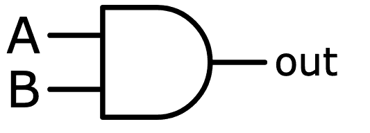
7408 IC Datasheet - AND Gate Pin Diagram and Truth Table
The 7408 IC is a quad 2-input AND gate integrated circuit. The 7408 datasheet shows it contains four independent AND gates in a single 14-pin DIP package. Each AND gate 7408 requires both inputs to be HIGH (1) for the output to be HIGH (1).
7408 IC Pin Configuration:
- Pin 1: 1A (Input)
- Pin 2: 1B (Input)
- Pin 3: 1Y (Output)
- Pin 4: 2A (Input)
- Pin 5: 2B (Input)
- Pin 6: 2Y (Output)
- Pin 7: GND
- Pin 8: 3Y (Output)
- Pin 9: 3A (Input)
- Pin 10: 3B (Input)
- Pin 11: 4Y (Output)
- Pin 12: 4A (Input)
- Pin 13: 4B (Input)
- Pin 14: VCC (+5V)
7408 Truth Table for each AND gate:
| Input A | Input B | Output Y |
|---|---|---|
| 0 | 0 | 0 |
| 0 | 1 | 0 |
| 1 | 0 | 0 |
| 1 | 1 | 1 |
7408 IC Specifications:
- Supply Voltage: 5V ±0.25V
- Operating Temperature: 0°C to 70°C
- Propagation Delay: 10ns typical
- Power Consumption: 10mW per gate
7432 IC Datasheet - OR Gate Pin Diagram and Truth Table
The 7432 IC is a quad 2-input OR gate integrated circuit. The 7432 datasheet shows it contains four independent OR gates in a single 14-pin DIP package. Each OR gate 7432 output will be HIGH (1) if at least one input is HIGH (1).
7432 IC Pin Configuration:
- Pin 1: 1A (Input)
- Pin 2: 1B (Input)
- Pin 3: 1Y (Output)
- Pin 4: 2A (Input)
- Pin 5: 2B (Input)
- Pin 6: 2Y (Output)
- Pin 7: GND
- Pin 8: 3Y (Output)
- Pin 9: 3A (Input)
- Pin 10: 3B (Input)
- Pin 11: 4Y (Output)
- Pin 12: 4A (Input)
- Pin 13: 4B (Input)
- Pin 14: VCC (+5V)
7432 Truth Table for each OR gate:
| Input A | Input B | Output Y |
|---|---|---|
| 0 | 0 | 0 |
| 0 | 1 | 1 |
| 1 | 0 | 1 |
| 1 | 1 | 1 |
7432 IC Specifications:
- Supply Voltage: 5V ±0.25V
- Operating Temperature: 0°C to 70°C
- Propagation Delay: 15ns typical
- Power Consumption: 10mW per gate
7404 IC Datasheet - NOT Gate Pin Diagram and Truth Table
The 7404 IC is a hex inverter (NOT gate) integrated circuit. The 7404 datasheet shows it contains six independent NOT gates in a single 14-pin DIP package. Each NOT gate 7404 inverts the input signal - when input is HIGH (1), output is LOW (0) and vice versa.
7404 IC Pin Configuration:
- Pin 1: 1A (Input)
- Pin 2: 1Y (Output)
- Pin 3: 2A (Input)
- Pin 4: 2Y (Output)
- Pin 5: 3A (Input)
- Pin 6: 3Y (Output)
- Pin 7: GND
- Pin 8: 4Y (Output)
- Pin 9: 4A (Input)
- Pin 10: 5Y (Output)
- Pin 11: 5A (Input)
- Pin 12: 6Y (Output)
- Pin 13: 6A (Input)
- Pin 14: VCC (+5V)
7404 Truth Table for each NOT gate:
| Input A | Output Y |
|---|---|
| 0 | 1 |
| 1 | 0 |
7404 IC Specifications:
- Supply Voltage: 5V ±0.25V
- Operating Temperature: 0°C to 70°C
- Propagation Delay: 12ns typical
- Power Consumption: 10mW per gate
7400 IC Datasheet - NAND Gate Pin Diagram and Truth Table
The 7400 IC is a quad 2-input NAND gate integrated circuit. The 7400 datasheet shows it contains four independent NAND gates in a single 14-pin DIP package. Each NAND gate 7400 is a combination of AND and NOT gates - output is LOW (0) only when both inputs are HIGH (1).
7400 IC Pin Configuration:
- Pin 1: 1A (Input)
- Pin 2: 1B (Input)
- Pin 3: 1Y (Output)
- Pin 4: 2A (Input)
- Pin 5: 2B (Input)
- Pin 6: 2Y (Output)
- Pin 7: GND
- Pin 8: 3Y (Output)
- Pin 9: 3A (Input)
- Pin 10: 3B (Input)
- Pin 11: 4Y (Output)
- Pin 12: 4A (Input)
- Pin 13: 4B (Input)
- Pin 14: VCC (+5V)
7400 Truth Table for each NAND gate:
| Input A | Input B | Output Y |
|---|---|---|
| 0 | 0 | 1 |
| 0 | 1 | 1 |
| 1 | 0 | 1 |
| 1 | 1 | 0 |
7400 IC Specifications:
- Supply Voltage: 5V ±0.25V
- Operating Temperature: 0°C to 70°C
- Propagation Delay: 10ns typical
- Power Consumption: 10mW per gate
7486 IC Datasheet - XOR Gate Pin Diagram and Truth Table
The 7486 IC is a quad 2-input XOR gate (Exclusive OR) integrated circuit. The 7486 datasheet shows it contains four independent XOR gates in a single 14-pin DIP package. Each XOR gate 7486 output is HIGH (1) when inputs are different (one HIGH, one LOW).
7486 IC Pin Configuration:
- Pin 1: 1A (Input)
- Pin 2: 1B (Input)
- Pin 3: 1Y (Output)
- Pin 4: 2A (Input)
- Pin 5: 2B (Input)
- Pin 6: 2Y (Output)
- Pin 7: GND
- Pin 8: 3Y (Output)
- Pin 9: 3A (Input)
- Pin 10: 3B (Input)
- Pin 11: 4Y (Output)
- Pin 12: 4A (Input)
- Pin 13: 4B (Input)
- Pin 14: VCC (+5V)
7486 Truth Table for each XOR gate:
| Input A | Input B | Output Y |
|---|---|---|
| 0 | 0 | 0 |
| 0 | 1 | 1 |
| 1 | 0 | 1 |
| 1 | 1 | 0 |
7486 IC Specifications:
- Supply Voltage: 5V ±0.25V
- Operating Temperature: 0°C to 70°C
- Propagation Delay: 17ns typical
- Power Consumption: 12mW per gate
Additional TTL Logic Gate ICs
For more advanced applications, consider these related ICs:
- IC 7402: Quad 2-input NOR gate datasheet
- IC 74266: Quad 2-input XNOR gate pin diagram
- IC 7407: Hex buffer datasheet
TTL Logic Gate Implementation and Circuit Design
Understanding TTL Logic Levels
TTL (Transistor-Transistor Logic) operates with specific voltage levels:
- Logic HIGH (1): 2.0V to 5.0V
- Logic LOW (0): 0V to 0.8V
- Undefined region: 0.8V to 2.0V (avoid this range)
IC Package Types and Mounting
These logic gate ICs are available in various packages:
- DIP (Dual In-line Package): 14-pin standard for breadboard use
- SOIC (Small Outline IC): Surface mount version
- TSSOP: Thin shrink small outline package
Power Supply Requirements
All 7400 series ICs require:
- VCC: +5V ±5% (pins 14)
- GND: 0V (pin 7)
- Decoupling capacitor: 0.1µF ceramic capacitor near VCC pin
Practical Applications and Circuit Examples
Building Complex Logic with Basic Gates
NAND gates (7400) are universal gates - you can build any logic function using only NAND gates:
- NOT gate: Connect both NAND inputs together
- AND gate: NAND followed by NOT
- OR gate: De Morgan's theorem implementation
Common Circuit Applications
- 7408 AND gate: Used in address decoding, enable signals
- 7432 OR gate: Used in interrupt handling, alarm systems
- 7404 NOT gate: Signal inversion, clock signal conditioning
- 7400 NAND gate: Universal building block for all logic
- 7486 XOR gate: Parity checking, data comparison
For hands-on experience with these TTL logic gate ICs, try our interactive logic gates simulator where you can build circuits using virtual 7408, 7432, 7404, 7400, and 7486 components and observe their behavior in real-time.